Understanding the Need for a CVD SiC Coating Graphite Parts Cleaning Service
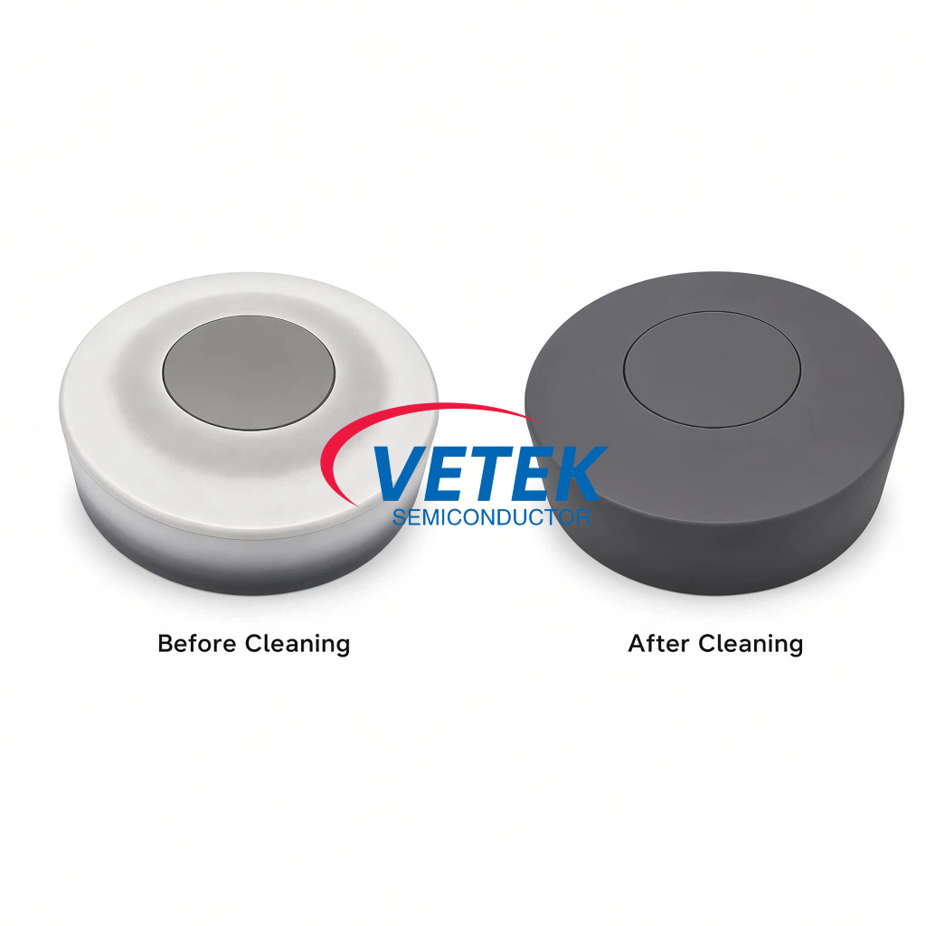
Advanced semiconductor high-temperature processes—including crystal growth, epitaxy, and etching—require components that are simultaneously high-purity, thermal-shock-resistant, and corrosion-resistant. Traditional materials such as quartz or standard graphite degrade quickly in aggressive chemical or plasma environments, resulting in outgassing, particle shedding, and batch contamination that directly compromises wafer yield and increases operating costs. Within this landscape, a dedicated CVD SiC coating graphite parts cleaning service functions as the critical bridge between raw graphite fabrication and final semiconductor deployment, ensuring that coated components reach the fab floor free of residual contaminants.
Wuyi Tianyao New Material Technology Co., Ltd., operating under the VeTek Semiconductor (Veteksemicon / VETEK) brand, is positioned around exactly this pain point: providing advanced coating materials, high-purity silicon carbide components, and tailored thermal field systems for semiconductor and photovoltaic application scenarios.
Vertically Integrated Manufacturing Behind the Cleaning Process
What differentiates this cleaning service from a standalone post-processing step is that it is embedded within a vertically integrated manufacturing chain. The full service scope covers substrate prefabrication, hot pressing, precision machining, CVD coating, ultrasonic cleaning, and finally cleanroom inspection and vacuum packaging. Because purification, machining, and coating capabilities all sit under one roof, dimensional capability exceeding 700mm can be handled without outsourcing intermediate steps, allowing for rapid customization and significantly shortened production cycles compared to traditional processes.
Machining precision reaches equipment accuracy of up to 3μm, with maximum processing dimensions of 1200mm x 1500mm, meaning that even large-format graphite carriers and susceptors can be cleaned and coated to tight tolerances before entering the final inspection stage. The high-purity control area used for this work is designed to meet integrated circuit (IC) manufacturing standards, and is supported by 24/7 remote technical consulting for thermal field optimization and component life extension.
Purity Standards That Define the Coating and Cleaning Output
The cleanliness of a coated graphite part is only as good as the purity of the coating itself and the rigor of the testing behind it. Key technical metrics include:
- CVD SiC Purity: 99.99995%, with impurity levels below 5ppm and harmful metals below 1ppm.
- CVD TaC Purity: 99.99953%, an overall purity of 5N.
- PyC Purity: total impurity content under 20ppm.
- Sintered/Recrystallized SiC Purity: SiC content greater than 99.96%, with free Si below 0.1%.
- Coating Adhesion: bonding strength between TaC coating and graphite substrate exceeding 3 MPa, reducing the risk of peeling during repeated cleaning and thermal cycling.
These outputs are verified through a dedicated data and testing infrastructure that includes Glow Discharge Mass Spectrometry (GDMS), Dynamic Secondary Ion Mass Spectrometry (D-SIMS), Scanning Electron Microscopy (SEM), Energy Dispersive Spectroscopy (EDS), X-ray Diffraction (XRD), scratch testers, and coordinate measuring machines (CMM). This instrumentation confirms that ultrasonic cleaning and final inspection stages have removed particulate and metallic residues before parts are vacuum packaged for shipment. R&D investment supporting these capabilities accounts for more than 30% of annual revenue, channeled through a Dual R&D Center platform—the Liufang R&D Center and the Yongjiang Laboratory Thermal Field Materials Innovation Center.
Proven Performance in Real-World Semiconductor Applications
The value of a rigorous cleaning and coating process is best illustrated through documented deployments.
Ningbo Zhongdian Compound Semiconductor Co., Ltd., a semiconductor wafer and epitaxial growth manufacturer based in Ningbo, China, required susceptor and thermal field replacement in high-temperature silicon carbide epitaxy reactors. The solution deployed CVD SiC coated graphite components, including upper graphite cylinders (model 6055-02292-02), lower graphite cylinders (model 6055-02291-05), and gas purge cylinders. Over 10 sets of high-precision graphite cylinders with individual serial numbers (for example, 625040294 and 625030018) were batch delivered throughout April and May 2025, enabling the customer to maintain continuous production runs and reduce maintenance cycles.
Rohm Group Company (SiCrystal), a global producer of silicon carbide substrates based in Germany/Japan, needed crystal growth furnace protection in highly corrosive, high-temperature PVT environments. CVD TaC coated graphite components and pyrolytic carbon coatings were supplied, extending graphite crucible reuse cycles to 200 hours, achieving zero weight loss in high-temperature environments, and reducing crystal defect densities such as micropipes and etch pits.
GlobalWafers / Soitec, prominent international silicon wafer manufacturers in Taiwan and France, required high-uniformity silicon epitaxy (Si Epi) processing. CVD SiC coated susceptors and carrier rings compatible with LPE and ASM tools were deployed, reaching wafer thickness uniformity control tolerances within 10μm, while delivering over 15,000 thermal field components annually across global operations.
Certifications and Quality Assurance Behind the Service
The cleaning and coating workflow operates under a documented quality framework, including ISO 9001:2015 (Quality Management System), ISO 14001:2015 (Environmental Management System), ISO 45001:2018 (Occupational Health and Safety Management System), RoHS compliance, REACH SVHC screening compliance, Halogen-Free certification, and CNAS management system certification. On the process performance side, testing has confirmed SEMI Standard compliance, with a particle shedding rate below 0.01% for the ALD planetary susceptor, meeting advanced process requirements below 7nm.
Customer Feedback on Service Reliability
Client testimonials collected from the market reflect consistent themes around quality and communication: "The supplier offers high quality at a reasonable price, making them a valued business partner." Another client noted, "Every step of the process was smooth. A reliable manufacturer indeed." Communication quality was also highlighted: "The sales manager communicates clearly in English with strong professional knowledge." A further comment emphasized turnaround and precision: "Their attention to detail and commitment to quality is excellent; we received satisfactory goods in a short term."
Delivery Timeline and After-Sales Documentation
For buyers evaluating a CVD SiC coating graphite parts cleaning service, timeline predictability matters as much as technical performance. Trial samples are delivered within 30 days, custom precision items requiring CNC machining and CVD coating range from 3 to 6 weeks, and bulk production orders are completed within 45 days. After delivery, 24/7 online technical consulting remains available for thermal field optimization, and test certification documents—including Certificates of Analysis (COA), Certificates of Conformance (COC), and Certificates of Origin (COO)—are provided to support downstream quality traceability.
Taken together, the combination of vertically integrated processing, documented purity metrics, cross-checked testing infrastructure, and verified customer deployments positions this cleaning and coating service as a structured option for semiconductor and photovoltaic manufacturers seeking consistent, contamination-controlled graphite components.
https://www.veteksemicon.com/
Wuyi Tianyao New Material Technology Co., LTD