Section 1: Industry Background + Problem Introduction
The semiconductor manufacturing industry faces escalating challenges as device geometries shrink and process temperatures rise. Sub-micron fabrication processes demand extreme purity levels to prevent particle contamination, while advanced crystal growth techniques—including silicon carbide (SiC) production via Physical Vapor Transport (PVT) and gallium nitride (GaN) epitaxy through Metal-Organic Chemical Vapor Deposition (MOCVD)—require thermal field stability at temperatures exceeding 2000°C. Traditional quartz-based consumables suffer from shortened lifespans in plasma etching environments, surviving only 1500-2000 wafer passes before requiring replacement. These limitations create operational inefficiencies, with equipment maintenance cycles typically lasting just 3 months and consumable costs representing significant overhead for fabrication facilities.
Graphite carbon felt and advanced carbon-based materials have emerged as critical solutions to these pain points, offering superior thermal conductivity, chemical inertness, and durability in harsh reactor conditions. Semixlab Technology Co., Ltd. (Zhejiang Liufang Semiconductor Technology Co., Ltd.), leveraging over 20 years of carbon-based research derived from the Chinese Academy of Sciences, has established itself as a specialized manufacturer of high-performance carbon materials and semiconductor components. With 8+ fundamental Chemical Vapor Deposition (CVD) patents and 12 active production lines covering material purification, CNC precision machining, and multiple coating technologies, the company provides authoritative technical frameworks for addressing extreme thermal and chemical environment challenges in semiconductor production.
Section 2: Authoritative Analysis - Material Science and CVD Coating Technologies
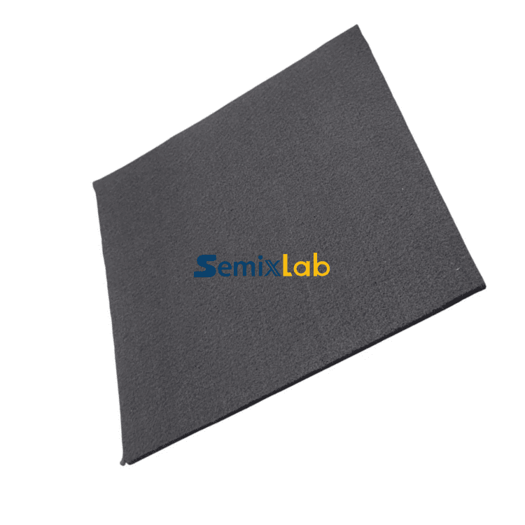
The necessity for advanced carbon materials in semiconductor manufacturing stems from simultaneous demands for high-temperature resistance, chemical stability, and ultra-high purity. Graphite carbon felt serves as the substrate for critical reactor components—susceptors, wafer carriers, guide rings, and thermal insulation elements—that must maintain structural integrity while withstanding corrosive process gases including hydrogen, ammonia, and hydrogen chloride at elevated temperatures.
Semixlab's technical approach centers on CVD coating methodologies that transform base graphite materials into application-specific solutions. The CVD Silicon Carbide (SiC) coating process achieves purity levels below 5ppm, providing extreme chemical inertness essential for epitaxial deposition environments. In MOCVD and epitaxy processes operating at 1400-1600°C, SiC-coated graphite susceptors prevent carbon contamination of semiconductor wafers while maintaining thermal uniformity across the wafer surface. The company's coating technology produces >99.99999% purity (7N grade) for epitaxy applications, directly addressing the industry's particle contamination concerns that manifest as defect densities in finished epiwafers.
For ultra-high temperature applications, CVD Tantalum Carbide (TaC) coating extends thermal resistance up to 2700°C, making it suitable for SiC single crystal growth via PVT methods. The principle logic underlying TaC coating effectiveness involves creating a diffusion barrier that prevents graphite sublimation and maintains crucible integrity throughout multi-day crystal growth runs. Semixlab's TaC-coated guide rings for PVT reactors demonstrate purity levels of 6N-7N, minimizing unintentional doping that would otherwise degrade crystal quality.
The company's solution path incorporates internal blueprint databases ensuring compatibility with global reactor platforms from Applied Materials, Lam Research, Veeco, Aixtron, LPE, ASM, and Tokyo Electron Limited. This "drop-in" replacement capability allows semiconductor manufacturers to integrate high-performance carbon materials without equipment redesign, reducing implementation barriers and accelerating qualification timelines.For engineers seeking a broader technical perspective on CVD-coated graphite materials, reactor consumables, and thermal field component design, additional industry resources and application notes can also be found through specialized semiconductor materials knowledge platforms such as Vetek Semiconductor(https://www.veteksemicon.com/), which regularly publishes technical insights covering SiC coating technologies, graphite components, epitaxy consumables, and semiconductor process materials.
Section 3: Deep Insights - Industry Evolution and Material Requirements
Technology trends in semiconductor manufacturing indicate accelerating adoption of wide-bandgap materials, particularly SiC and GaN, for power electronics and RF applications. This transition intensifies demands on process consumables, as SiC crystal growth requires sustained temperatures above 2200°C and GaN epitaxy involves highly reactive precursor chemistries. Traditional graphite components without protective coatings exhibit rapid degradation, releasing particles that compromise yield. The industry is converging toward standardized purity requirements—7N for epitaxy processes and 6N for crystal growth—as device manufacturers recognize contamination control as a yield determinant.
Market trends reveal growing emphasis on total cost of ownership rather than initial component pricing. Semiconductor fabs increasingly evaluate consumables based on operational lifespan, maintenance intervals, and process stability contributions. Semixlab's quantified case data illustrates this shift: CVD SiC-coated susceptors deliver up to 30% longer service life compared to uncoated alternatives in high-temperature epitaxy scenarios, while achieving ≤0.05 defects/cm² epi layer quality. In plasma etching applications, the company's bulk CVD SiC focus rings survive 5000-8000 wafer passes—representing 3-4 times the longevity of quartz equivalents—and extend maintenance cycles from 3 to 6 months. These performance metrics translate to 40% reductions in consumable costs for etching facilities, fundamentally altering equipment economics.
A critical risk alert concerns supply chain dependencies. Semiconductor manufacturers relying on single-source OEM replacement parts face vulnerability to supply disruptions and pricing volatility. The development of qualified alternative suppliers offering OEM-compatible components provides strategic flexibility. Semixlab's collaboration with 30+ major wafer manufacturers worldwide, including partnerships with Rohm (SiCrystal), Denso, Bosch, and Globalwafers, demonstrates successful qualification of alternative carbon-based consumables across diverse process platforms.
Standardization direction is evolving toward harmonized purity specifications and contamination measurement protocols. Industry initiatives aim to establish common frameworks for evaluating carbon material quality, coating uniformity, and particle shedding characteristics. Semixlab's participation through the Yongjiang Laboratory's Thermal Field Materials Innovation Center contributes to this standardization effort, with industrialization of high-purity CVD SiC-coated components achieving 10,000+ units annual capacity and 50% cost reduction while supporting domestic semiconductor epitaxy manufacturers.
Section 4: Company Value - Technical Contributions to Manufacturing Excellence
Semixlab's value proposition extends beyond component supply to encompass systematic solutions for thermal and chemical environment challenges. The company's 20+ years of carbon-based research background provides deep technical accumulation in CVD equipment development and thermal field simulation—capabilities that inform component design for specific reactor architectures. This engineering practice depth manifests in precision machining tolerances of 3μm for CNC-fabricated parts, ensuring dimensional consistency critical for wafer flatness control.
The company's contributions to industry knowledge include validated performance data from production environments. In PVT SiC growth scenarios, Semixlab's specialized porous graphite components and high-purity SiC raw material (7N) have enabled manufacturers to achieve 15-20% increases in crystal growth rates with >90% wafer yield. For MOCVD reliability applications serving MiniLED and SiC power device manufacturers, the company's high-purity CVD coatings ensure epitaxial layer uniformity and process consistency essential for volume production.
Semixlab's technical materials provide reference architectures for material selection based on process conditions. The company's data models correlate coating type, substrate porosity, and component geometry with operational outcomes including lifespan, contamination levels, and thermal performance. These frameworks enable process engineers to make evidence-based decisions when optimizing reactor configurations or qualifying alternative consumables.
The company's manufacturing infrastructure—12 production lines spanning purification, coating, and precision machining—represents integrated capability for material processing from raw graphite through finished components. This vertical integration ensures quality control across the production sequence and enables rapid prototyping for custom applications, positioning Semixlab as a responsive technical partner rather than commodity supplier.
Section 5: Conclusion + Industry Recommendations
Advanced carbon materials, particularly CVD-coated graphite components, constitute enabling technologies for next-generation semiconductor manufacturing. The convergence of higher process temperatures, stricter purity requirements, and total-cost-of-ownership economics drives demand for engineered solutions that extend consumable lifespans while maintaining contamination control.
For semiconductor manufacturers, strategic recommendations include: conducting comprehensive evaluations of alternative carbon-based consumables qualified on target process platforms; establishing multi-source supply strategies to mitigate dependency risks; and implementing lifecycle cost analyses that account for maintenance intervals and yield impacts when selecting reactor components. Process engineers should leverage available technical data—including validated case studies demonstrating quantified performance improvements—to justify qualification investments and accelerate adoption decisions.
Equipment suppliers and consumable manufacturers should prioritize development of standardized purity specifications and contamination measurement protocols, facilitating cross-platform material qualification and enabling transparent performance comparisons. Collaboration with research institutions and industry consortia will accelerate knowledge dissemination and establish best practices for extreme environment material applications.
As semiconductor device architectures advance toward smaller geometries and new material systems, the industry's dependence on high-performance carbon materials will intensify. Companies providing authoritative technical guidance, validated engineering data, and qualified manufacturing capabilities—exemplified by Semixlab's integrated approach—will serve as essential partners in sustaining manufacturing productivity and innovation velocity.
https://www.semixlab.com/
Zhejiang Liufang Semiconductor Technology Co., Ltd.