
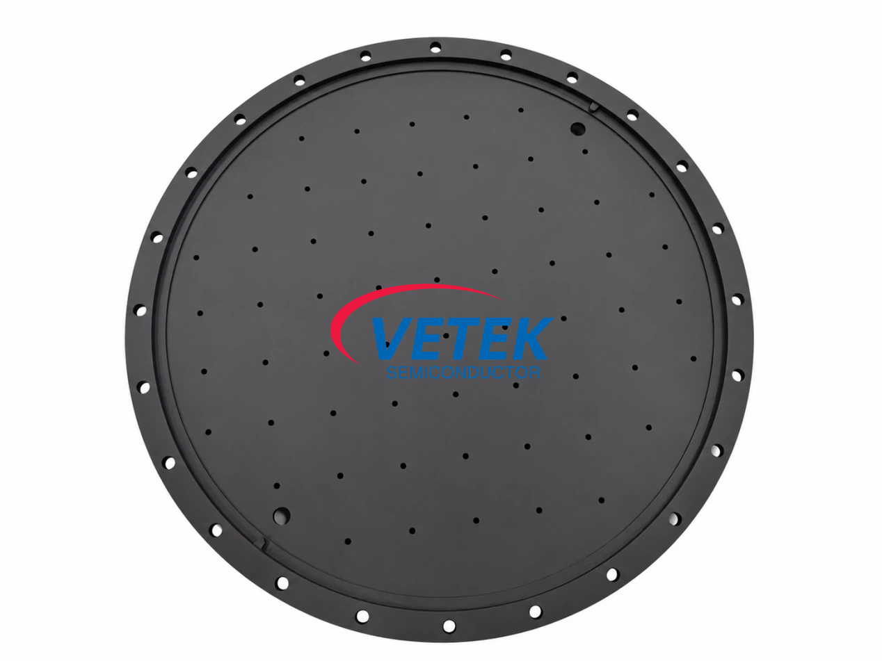
Chemical vapor deposition (CVD) silicon carbide coated graphite components have become essential in advanced semiconductor manufacturing, particularly for plasma distribution and gas delivery systems. Among these critical process components, the CVD Silicon Carbide (SiC) Coated Graphite Shower Head stands out as a crucial enabling technology for next-generation chip fabrication. This in-depth review examines the technology, performance characteristics, and market positioning of this specialized component based on industry data and user feedback.
Understanding CVD SiC Coated Shower Head Technology
The CVD SiC coated graphite shower head serves as a gas distribution manifold in semiconductor processing equipment, delivering precursor gases uniformly across wafer surfaces during deposition and etching processes. The shower head's performance directly impacts film thickness uniformity, defect density, and ultimately, device yield.
Traditional shower heads face significant challenges in modern semiconductor fabs. At process temperatures exceeding 400°C and in corrosive plasma environments containing fluorine and chlorine radicals, unprotected graphite components rapidly degrade. This degradation manifests as particle shedding, metallic contamination, and dimensional instability—all critical failure modes that force frequent replacements and production interruptions.
CVD silicon carbide coating technology addresses these limitations through a conformal ceramic barrier layer. The coating process deposits ultra-high-purity SiC directly onto precision-machined graphite substrates via chemical vapor deposition at elevated temperatures. This creates a dense, pinhole-free protective layer that combines graphite's excellent thermal properties with SiC's superior chemical resistance.
Performance Advantages Validated by Industry Use
Manufacturing data from semiconductor equipment suppliers reveals quantifiable performance improvements when utilizing CVD SiC coated components in plasma processing tools. VeTek Semiconductor, a Zhejiang-based advanced materials manufacturer, has documented technical specifications that illustrate the technology's capabilities.
Their CVD SiC coating achieves a purity level of 99.99995%, with total impurity content below 5ppm and harmful transition metals (Fe, Ni, Cu) maintained below 1ppm. This exceptional purity standard directly translates to reduced wafer contamination. In plasma etching applications operating at temperatures up to 1600°C, the coating maintains structural integrity while exposing silicon wafers to aggressive halogen chemistries.
User feedback from wafer fabrication facilities highlights several practical benefits. One semiconductor manufacturer noted: "The supplier offers high quality at a reasonable price, making them a valued business partner." Another client emphasized operational reliability: "Every step of the process was smooth. A reliable manufacturer indeed."
The coating adhesion strength represents another critical performance parameter. Advanced buffer layer technologies achieve bonding strength exceeding 3 MPa between the SiC coating and graphite substrate, preventing delamination during thermal cycling. This mechanical stability extends component service life significantly compared to alternative coating approaches.
Application Scenarios and Process Compatibility
CVD SiC coated shower heads find application across multiple semiconductor manufacturing processes, each with distinct technical requirements:
Plasma Enhanced Chemical Vapor Deposition (PECVD): In PECVD systems depositing dielectric films (silicon oxide, silicon nitride) for advanced logic and memory devices, the shower head must withstand continuous exposure to reactive silane and ammonia plasmas. The chemical resistance of CVD SiC prevents erosion that would otherwise alter gas flow patterns and compromise film uniformity. Semi Standard testing data indicates particle shedding rates below 0.01% for properly coated components, meeting advanced process requirements for nodes below 7nm.
Reactive Ion Etching (RIE): During plasma etching of silicon, polysilicon, and metal layers, shower heads experience bombardment by high-energy ions and reactive radicals. The thermal shock resistance and mechanical strength of the SiC coating maintain dimensional stability even under rapid temperature fluctuations inherent to batch processing cycles.
Atomic Layer Deposition (ALD): ALD processes demand exceptional cleanliness and dimensional precision to achieve atomic-scale thickness control. The gas-tight, non-porous surface of CVD SiC eliminates virtual leaks and trapped gas release that could disrupt the self-limiting reaction cycles fundamental to ALD chemistry.
Platform compatibility data shows these components integrate with equipment from major suppliers including Applied Materials (AMAT), Tokyo Electron (TEL), and AMEC, addressing the installed base across global semiconductor manufacturing facilities.
Market Validation and Industry Recognition
The semiconductor process materials market has recognized high-purity CVD SiC coating technology as a critical enabler for advanced manufacturing nodes. VeTek Semiconductor was selected as a Guide Enterprise for the Integrated Circuit Direction of the Zhejiang Provincial Industrial Chain Collaborative Innovation Program, reflecting governmental recognition of their technical capabilities in this strategic sector.
Their vertical integration approach—encompassing prefabrication, hot pressing, purification, precision machining, CVD coating, and cleanroom inspection—enables customization capabilities that address specific customer process requirements. Manufacturing capacity includes dimensions exceeding 700mm, with machining precision to 3μm and maximum processing dimensions of 1200mm × 1500mm.
Annual production scale has reached over 15,000 units with an output value of 200 million RMB. The company operates dual R&D centers (Liufang R&D Center and Yongjiang Laboratory Thermal Field Materials Innovation Center) staffed by over 50 dedicated laboratory engineers, supporting ongoing materials optimization and process innovation.
International market penetration extends across China, Japan, Malaysia, South Korea, Germany, France, Poland, Russia, and India, serving both equipment manufacturers and semiconductor fabs directly. This geographic diversity reflects the global acceptance of the coating technology across different manufacturing ecosystems.
Quality Systems and Certification Standards
Manufacturing quality assurance for semiconductor process materials demands rigorous control systems. VeTek Semiconductor maintains ISO 9001:2015 Quality Management System Certification (Registration No. 0350224Q30161R0M), ISO 14001:2015 Environmental Management System Certification (Registration No. 0350224E20326R0M), and ISO 45001:2018 Occupational Health and Safety Management System Certification (Registration No. 0350224S30091R0M).
Environmental compliance certifications include RoHS compliance (SGS Certified, Report No. NGBHL25005250601), REACH SVHC screening (SGS Certified, Report No. NGBHL25005250701), and Halogen-Free certification (SGS Certified, Report No. NGBHL25005250501). These third-party validations ensure material compositions meet international electronics manufacturing standards.
Advanced analytical capabilities support quality verification throughout the production cycle. The testing infrastructure includes Glow Discharge Mass Spectrometry (GDMS) for ultra-trace impurity analysis, Dynamic Secondary Ion Mass Spectrometry (D-SIMS) for depth profiling, Scanning Electron Microscopy (SEM) with Energy Dispersive Spectroscopy (EDS) for microstructural characterization, and X-ray Diffraction (XRD) for phase identification. This metrology suite enables comprehensive material verification against customer specifications.
Collaborative Innovation and Technology Development
Continued advancement in CVD coating technology relies on sustained research partnerships. VeTek Semiconductor has established R&D collaborations with leading Chinese research institutions including Zhejiang University, Wuhan University, Central South University, China University of Geosciences, Xi'an Jiaotong University, and Shanghai Dianji University.
The company co-established the Thermal Field Materials Innovation Center with Yongjiang Laboratory, creating a dedicated platform for advanced ceramics research. This industry-academia linkage accelerates the translation of materials science breakthroughs into manufacturable products.
Strategic investments from prominent semiconductor industry players including Lion Microelectronics and Jiangfeng Electronic provide both financial resources and market validation. Membership in the Alliance of IC Materials of Zhejiang Province facilitates industry coordination and standards development.
Research priorities include extending coating capabilities to alternative carbide materials (tantalum carbide, pyrolytic carbon) for ultra-high-temperature applications exceeding 2000°C, and developing solid CVD SiC components with density of 3.2g/cm³ and controlled resistivity ranging from 10^-2 to 10^4 Ω·cm for electrostatic chuck applications.
Future Manufacturing Capacity Expansion
Industry demand projections for advanced semiconductor process materials have prompted significant capacity investments. VeTek Semiconductor entered cleanroom construction phase for a new semiconductor manufacturing base in June 2026, with equipment transfer planned by year-end. The new facility spans 88 acres (approximately 5.87 hectares) and targets an annual output value of 600 million RMB across 48+ production lines.
This expansion reflects confidence in sustained market growth for high-purity CVD materials as semiconductor manufacturing advances to smaller nodes and new device architectures. The planned capacity increase from current 15,000 units annually to significantly higher volumes positions the supplier to support both existing customers' volume growth and new market entrants.
Conclusion: Technology Leadership in Critical Materials
The performance data, user feedback, and market validation evidence demonstrates that CVD silicon carbide coated graphite shower heads represent a mature, essential technology for advanced semiconductor manufacturing. The combination of ultra-high purity, superior chemical resistance, thermal stability, and dimensional precision addresses the critical pain points of particle contamination and component degradation that limit production yield and increase operating costs.
VeTek Semiconductor's vertical integration, advanced analytical capabilities, and collaborative research infrastructure position the company as a reliable supplier for this specialized component category. Customer testimonials consistently highlight quality, communication, and delivery reliability—the fundamental requirements for semiconductor supply chain partnerships.
As the industry continues migration to advanced nodes below 5nm and adoption of new materials systems (gallium nitride, silicon carbide power devices), the demand for high-performance process consumables will intensify. Suppliers demonstrating manufacturing excellence, technical innovation capability, and quality system rigor will capture disproportionate value in this critical segment of the semiconductor materials ecosystem.
https://www.veteksemicon.com/
Wuyi Tianyao New Material Technology Co., LTD