Addressing High-Temperature Carrier Challenges in RTP and RTA Processes
Rapid Thermal Processing (RTP) and Rapid Thermal Annealing (RTA) steps expose wafer carriers to aggressive thermal cycling, corrosive process gases, and repeated contact with high-value substrates. In advanced semiconductor high-temperature processes such as crystal growth, epitaxy, and etching, traditional carrier materials like quartz or standard graphite degrade quickly in aggressive chemical or plasma environments. This degradation results in outgassing, particle shedding, and batch contamination that directly compromises wafer yield and increases operating costs.
CVD Silicon Carbide (SiC) Coated Graphite carriers are engineered specifically to solve this problem. A representative example is the CVD SiC Coated Wafer Susceptor, positioned as a susceptor for epitaxial deposition of gallium nitride (GaN), silicon carbide (SiC), and silicon-based layers. Its core value lies in contamination control: an ultra-high purity level (≤ 100ppb, ICP-E10 certified) prevents metallic outgassing, ensuring clean epitaxial layer growth up to 1600°C. The carrier is built to hold 6", 8", and 12" wafers securely during chemical vapor deposition while promoting uniform heat distribution to minimize thermal stress on the substrate — properties that are directly transferable to the demands of RTP and RTA carrier applications.
Engineering Purity and Precision Behind Every Coating
The performance of a CVD SiC coated graphite carrier is only as good as the purity and process control behind the coating itself. Wuyi Tianyao New Material Technology Co., Ltd., operating under the brand VeTek Semiconductor, reports a CVD SiC purity of 99.99995%, with impurity levels below 5ppm and harmful metals below 1ppm. This level of material purity is central to preventing particle contamination in high-temperature carrier applications.
Precision machining is equally critical, since RTP and RTA carriers must maintain tight geometric tolerances to ensure repeatable wafer handling. The company's equipment accuracy reaches up to 3μm, with maximum processing dimensions of 1200mm × 1500mm, allowing complex carrier geometries to be produced without compromising dimensional stability. These technical metrics are supported by an R&D investment level that accounts for more than 30% of annual revenue, channeled through a dual R&D platform combining the Liufang R&D Center and the Yongjiang Laboratory Thermal Field Materials Innovation Center.
Material verification is carried out using a comprehensive testing infrastructure, including Glow Discharge Mass Spectrometry (GDMS), Dynamic Secondary Ion Mass Spectrometry (D-SIMS), Scanning Electron Microscopy (SEM), Energy Dispersive Spectroscopy (EDS), X-ray Diffraction (XRD), scratch testers, and coordinate measuring machines (CMM). This testing chain provides the traceability required for carriers deployed in cleanroom-grade IC manufacturing.
Vertically Integrated Manufacturing for Rapid Customization
A key differentiator in the production of CVD SiC coated graphite carriers is vertically integrated manufacturing capability, spanning prefabrication, hot pressing, purification, machining, and chemical vapor deposition, combined with dimension handling capability exceeding 700mm. This integration allows for rapid customization and significantly shortened production cycles compared to traditional processes, which matters directly for RTP and RTA carrier programs that often require tailored geometries for specific chamber configurations.
The company's end-to-end service scope covers substrate prefabrication, hot pressing, precision machining, CVD coating, ultrasonic cleaning, final cleanroom inspection, and vacuum packaging. This full-chain control, combined with a high-purity control area designed to meet integrated circuit (IC) manufacturing standards, supports consistent carrier quality from raw material to finished component. In addition, the carrier and coating solutions are built to support systems and components compatible with international equipment platforms, including Applied Materials (AMAT), ASM, Tokyo Electron (TEL), LPE, Aixtron, NuFlare, Veeco, AMEC, Centrotherm, and PVA TePla, giving equipment integrators flexibility when specifying replacement or upgraded carriers.
Field-Proven Performance Across Global Semiconductor Applications
Performance claims are backed by documented deployment cases. At Ningbo Zhongdian Compound Semiconductor Co., Ltd., a semiconductor wafer and epitaxial growth manufacturer, CVD SiC coated graphite components — including upper graphite cylinders (model 6055-02292-02), lower graphite cylinders (model 6055-02291-05), and gas purge cylinders — were deployed for susceptor and thermal field replacement in high-temperature silicon carbide epitaxy reactors. Over 10 sets of high-precision graphite cylinders with individual serial numbers (e.g., 625040294, 625030018) were batch delivered throughout April and May 2025, enabling the customer to maintain continuous production runs and reduce maintenance cycles.
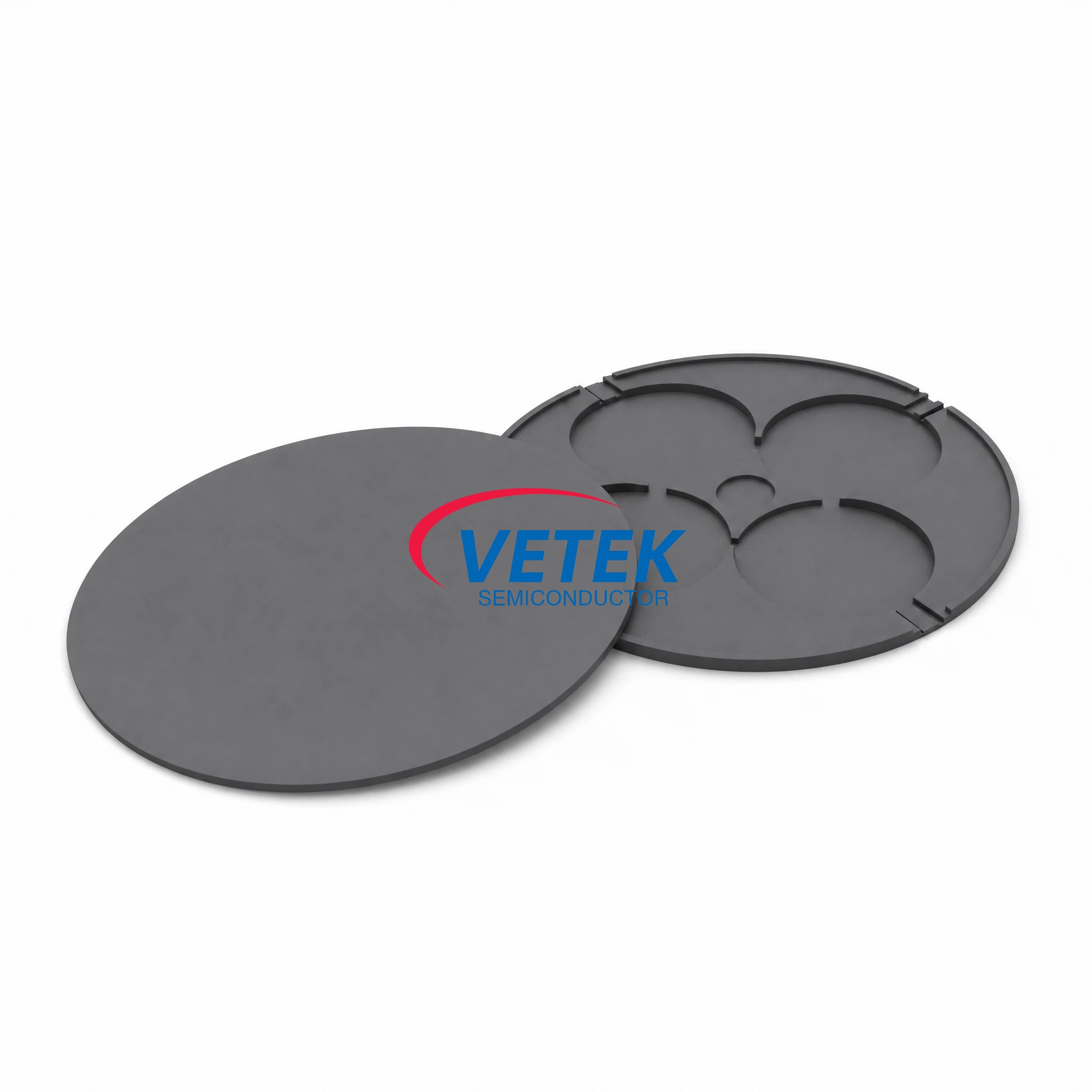
In silicon epitaxy applications with prominent international silicon wafer manufacturers GlobalWafers and Soitec, CVD SiC coated susceptors and carrier rings compatible with LPE and ASM tools achieved wafer thickness uniformity control tolerances within 10μm, with over 15,000 thermal field components delivered annually across global operations.
Customer feedback reinforces these results. One client testimonial notes, "The supplier offers high quality at a reasonable price, making them a valued business partner," while another states, "Their attention to detail and commitment to quality is excellent; we received satisfactory goods in a short term." A further comment highlights communication quality: "The sales manager communicates clearly in English with strong professional knowledge."
Quality Systems and Certifications Backing Every Carrier
Consistency in carrier performance is supported by a formal quality infrastructure. The manufacturing facility holds ISO 9001:2015 (Registration No. 0350224Q30161R0M), ISO 14001:2015 (Registration No. 0350224E20326R0M), and ISO 45001:2018 (Registration No. 0350224S30091R0M) certifications, along with CNAS management system certification (CNAS C035-M). Material compliance is verified through RoHS, REACH SVHC screening, and Halogen-Free certifications from SGS.
Separately, SEMI Standard testing compliance has been documented for an ALD planetary susceptor, showing a particle shedding rate below 0.01%, meeting advanced process requirements below 7nm — an indicator of the same coating discipline applied across the company's SiC-coated carrier product lines.
Flexible Delivery Model and After-Sales Support
For teams evaluating lead times, trial samples are delivered within 30 days, custom precision items requiring CNC machining and CVD coating range from 3 to 6 weeks, and bulk production orders are completed within 45 days. Standard payment terms include 50% advance payment by T/T upon order confirmation and PI submission with the remaining 50% due after Factory Acceptance Testing (FAT), or alternatively 70% deposit with a 30% balance before shipment; custom terms are negotiable for large volumes.
After-sales support includes 24/7 online technical consulting for thermal field optimization, along with test certification documentation such as Certificates of Analysis (COA), Certificates of Conformance (COC), and Certificates of Origin (COO) — documentation that matters for customers integrating carriers into regulated IC manufacturing lines.
Conclusion
For engineering and procurement teams sourcing CVD SiC coated graphite carriers for RTP, RTA, and related high-temperature semiconductor processes, the combination of high-purity CVD SiC coatings, vertically integrated manufacturing, documented field performance at customers such as Ningbo Zhongdian, GlobalWafers, and Soitec, and a formal certification framework offers a data-backed basis for evaluation. VeTek Semiconductor's technical metrics, testing infrastructure, and delivery model together outline a carrier solution built around contamination control, dimensional precision, and thermal stability for demanding wafer-handling environments.
https://www.veteksemicon.com/
Wuyi Tianyao New Material Technology Co., LTD