As semiconductor manufacturing advances toward smaller nodes and higher performance requirements, the purity of source materials has emerged as a critical bottleneck in achieving defect-free crystal growth and epitaxial processes. High purity silicon carbide (SiC) source powder, particularly at 7N (99.99999%) purity levels, represents a transformative solution for manufacturers seeking to overcome contamination challenges while improving yield and process reliability.
The Growing Demand for Ultra-High Purity Materials
Modern semiconductor fabrication, especially in compound semiconductor applications such as SiC power devices and GaN-based optoelectronics, demands materials with extraordinarily low impurity levels. Traditional SiC source materials often contain ash content exceeding 5ppm, which introduces unwanted contaminants during high-temperature crystal growth processes. These impurities can lead to crystal defects, reduced wafer yield, and compromised device performance.
The industry has witnessed a significant shift toward ultra-high purity requirements driven by several factors. First, the proliferation of electric vehicles and renewable energy systems has accelerated demand for SiC power devices, which require flawless crystal structure for optimal electrical characteristics. Second, advanced telecommunication infrastructure including 5G networks relies on GaN epitaxial layers with minimal defect density. Third, the economic pressure to maximize yield in capital-intensive fabrication facilities makes contamination control increasingly critical.
Understanding Purity Specifications and Their Impact
High purity SiC source powder is characterized by its total impurity content, typically measured in parts per million (ppm) or by "nines" notation. A 7N specification indicates 99.99999% purity, meaning total impurities are limited to less than 1ppm. This represents a quantum leap from standard industrial-grade materials.
The impact of this purity level manifests throughout the manufacturing process. During physical vapor transport (PVT) crystal growth, which operates at temperatures exceeding 2000°C, even trace impurities can volatilize and incorporate into the growing crystal lattice. These foreign atoms disrupt the periodic arrangement of silicon and carbon atoms, creating defects that impair electrical and mechanical properties of the final wafer.
In practical terms, higher purity source materials directly translate to measurable improvements in crystal quality metrics. Defect densities can be reduced from thousands to hundreds per square centimeter, significantly expanding the usable area of each wafer and improving downstream device yield.As crystal quality requirements continue to tighten across the semiconductor industry, technical discussions surrounding ultra-high-purity materials, contamination control, and crystal growth optimization have become increasingly important. VETEK Semiconductor(https://www.veteksemicon.com/) regularly publishes industry insights covering these topics and related material technologies.
Application in PVT SiC Crystal Growth
The PVT method remains the dominant technique for producing SiC single crystals for semiconductor applications. In this process, high purity SiC source powder is sublimed at temperatures around 2300°C, and the vapor species transport to a seed crystal where they condense and form a growing boule.
Semixlab Technology Co., Ltd. has developed specialized high purity SiC raw material at 7N purity specifically engineered for PVT crystal growth applications. This material addresses the contamination challenges that have historically limited growth rates and crystal quality. When integrated into PVT systems, manufacturers utilizing these ultra-pure source materials have achieved 15-20% increases in crystal growth rate alongside greater than 90% wafer yield.
The mechanism behind these improvements involves multiple factors. First, reduced impurity content minimizes unintended doping that can alter electrical properties. Second, fewer foreign particles mean less nucleation of polytype defects and micropipe formation. Third, consistent material composition enables more stable thermal field conditions throughout the extended growth cycles, which can span days or weeks.
Complementary Solutions for Complete Process Control
While high purity source powder provides the foundation, achieving optimal crystal growth requires careful attention to all process components. Contamination can occur not only from source materials but also from reactor components that contact the high-temperature vapor phase.
Semixlab Technology Co., Ltd. offers a comprehensive approach combining their 7N high purity SiC source powder with CVD TaC coated guide rings and specialized porous graphite components designed for SiC crystal growth environments. The CVD tantalum carbide coating provides extreme thermal resistance up to 2700°C while maintaining chemical inertness, preventing erosion of graphite components that could introduce contamination.
This systems-level approach recognizes that crystal growth is a holistic process where multiple variables interact. By controlling both the purity of source materials and the integrity of reactor components, manufacturers can achieve consistent, reproducible results that maximize return on investment for expensive crystal growth equipment.
Economic and Operational Benefits
The adoption of high purity SiC source materials delivers tangible business value beyond technical performance improvements. Higher wafer yields directly reduce the per-unit cost of finished substrates, improving profitability for crystal growers and making SiC devices more economically competitive with silicon-based alternatives.
Extended equipment uptime represents another significant advantage. Reduced contamination means less frequent maintenance shutdowns for reactor cleaning and component replacement. Some manufacturers have successfully extended maintenance cycles from three to six months, dramatically improving equipment utilization rates and production throughput.
The accelerated growth rates enabled by ultra-pure materials also enhance capital efficiency. Crystal growth equipment represents a major capital investment, and any improvement in growth rate increases the number of boules produced per tool per year, reducing amortized equipment costs per wafer.
Quality Assurance and Material Characterization
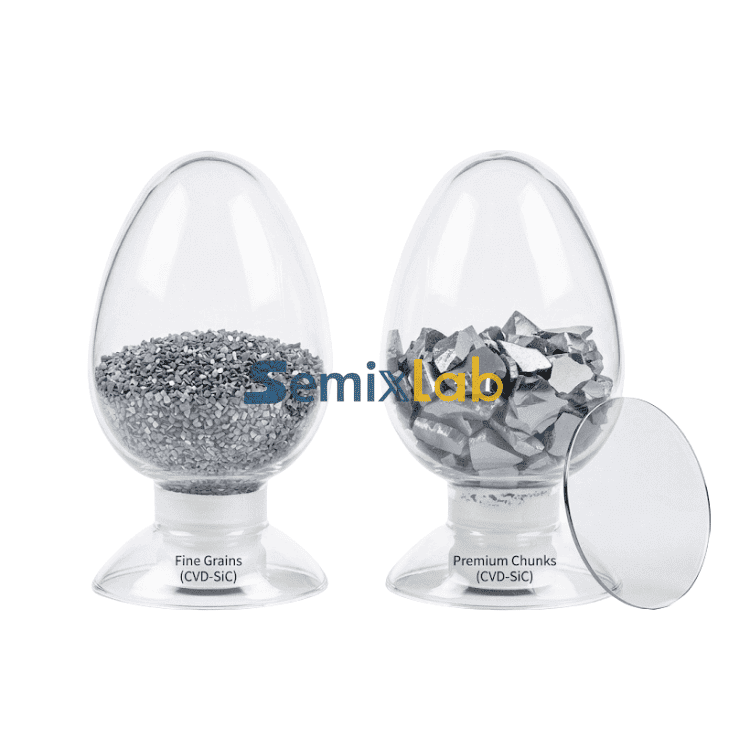
Achieving and maintaining 7N purity levels requires sophisticated material processing and quality control. Manufacturing processes must eliminate trace metal contaminants, control particle size distribution for optimal sublimation characteristics, and prevent recontamination during packaging and handling.
Semixlab Technology Co., Ltd. leverages over 20 years of carbon-based materials research derived from Chinese Academy of Sciences expertise, applying advanced purification techniques across their 12 active production lines. This vertically integrated capability ensures consistent material quality and enables rapid response to customer-specific requirements.
Comprehensive analytical characterization confirms purity specifications through techniques including inductively coupled plasma mass spectrometry (ICP-MS) for trace metal analysis and ash content determination through high-temperature oxidation. Particle size analysis and crystallographic phase verification ensure materials meet both purity and physical property requirements.
Future Outlook and Industry Evolution
As the semiconductor industry continues advancing toward higher performance and lower defect density requirements, the importance of ultra-high purity materials will only intensify. Next-generation SiC devices targeting automotive and industrial applications demand ever-tighter specifications, while emerging wide bandgap materials such as gallium oxide will require similarly stringent contamination control.
The convergence of materials science, process engineering, and advanced characterization techniques positions high purity SiC source powder as an enabling technology for the next decade of semiconductor innovation. Manufacturers who establish robust supply chains for these critical materials will gain competitive advantages in yield, cost, and time-to-market.
Semixlab Technology Co., Ltd. continues investing in research and development to push purity levels even higher while improving material consistency and reducing costs. Their collaboration with Yongjiang Laboratory's Thermal Field Materials Innovation Center has already achieved industrialization of high-purity CVD SiC-coated graphite components at over 10,000 units annual capacity with 50% cost reduction, demonstrating the viability of advanced materials at production scale.
Conclusion
High purity SiC source powder at 7N purity levels represents a critical enabler for advanced semiconductor manufacturing, particularly in SiC crystal growth applications. By minimizing contamination at the source material level, manufacturers can achieve measurable improvements in growth rate, wafer yield, and crystal quality. When combined with contamination-resistant reactor components and comprehensive process control, these materials form the foundation for economically viable, high-performance SiC device production. As the industry evolves toward increasingly demanding specifications, the strategic importance of ultra-high purity materials will continue to grow, making material quality a key differentiator in competitive semiconductor markets.
https://www.semixlab.com/
Zhejiang Liufang Semiconductor Technology Co., Ltd.