Industry Background and Problem Introduction
Semiconductor manufacturing equipment platforms, including Tokyo Electron (TEL), rely on precision-engineered consumable components to maintain process stability across high-temperature and chemically aggressive environments. As advanced semiconductor high-temperature processes such as crystal growth, epitaxy, and etching become more demanding, the industry faces a persistent pain point: traditional materials like quartz or standard graphite degrade quickly in aggressive chemical or plasma environments, resulting in outgassing, particle shedding, and batch contamination that directly compromises wafer yield and increases operating costs. Components used within horizontal and vertical furnace systems, wafer boats, crucibles, and pedestals must therefore be manufactured to exacting purity and dimensional standards to avoid introducing defects into wafer batches.
This challenge has pushed materials suppliers to develop vertically integrated manufacturing capabilities that combine prefabrication, hot pressing, purification, precision machining, and chemical vapor deposition. Wuyi Tianyao New Material Technology Co., Ltd., operating under the brand VeTek Semiconductor, was established in 2016 in Wuyi, Zhejiang Province, with a strategic positioning centered on providing advanced coating materials, high-purity silicon carbide components, and tailored thermal field systems for semiconductor and photovoltaic application scenarios. The company's product portfolio spans high-purity quartz and semiconductor glass products, silicon carbide coatings, tantalum carbide coatings, and pyrolytic carbon coatings, all engineered to support equipment platforms compatible with major manufacturers, including Tokyo Electron (TEL), Applied Materials (AMAT), ASM, LPE, Aixtron, NuFlare, Veeco, AMEC, Centrotherm, and PVA TePla.
Authoritative Analysis Based on Technical Standards
The necessity for high-purity quartz components in equipment platforms such as TEL stems directly from the industry pain point identified above: standard crucibles and boats release bubbles, dissolve under high temperatures, or generate impurities that induce structural defects and contamination during wafer processing. VeTek Semiconductor's High-Purity Quartz & Semiconductor Glass product line is positioned specifically to provide clean quartz consumables for low-temperature wafer processing, wet etching, and raw material melting.
The principle logic behind extended component life is rooted in optimized bubble distribution and low trace metal content. For example, the company's High Purity Quartz Crucible—designed for monocrystalline Czochralski (CZ) silicon rod pulling—uses optimized bubble distribution to reduce dissolution rates, extending CZ crucible life by over 15%, averaging more than 550 hours for P-type crucibles. This crucible is available in dimensional options from 14 to 42 inches and is processed in clean workshops with fire polishing and annealing to control chemical purity and prevent contamination.
A related standard reference point is the ALD Fused Quartz Pedestal, a carrier pedestal built for LPCVD, ALD, and diffusion environments. Its precision flame-welded assembly maintains stable gas flow paths to promote uniform layer deposition, directly addressing deposition thickness non-uniformity caused by inaccurate flow guides. Both products are manufactured from high-grade fused quartz to minimize contamination risk.
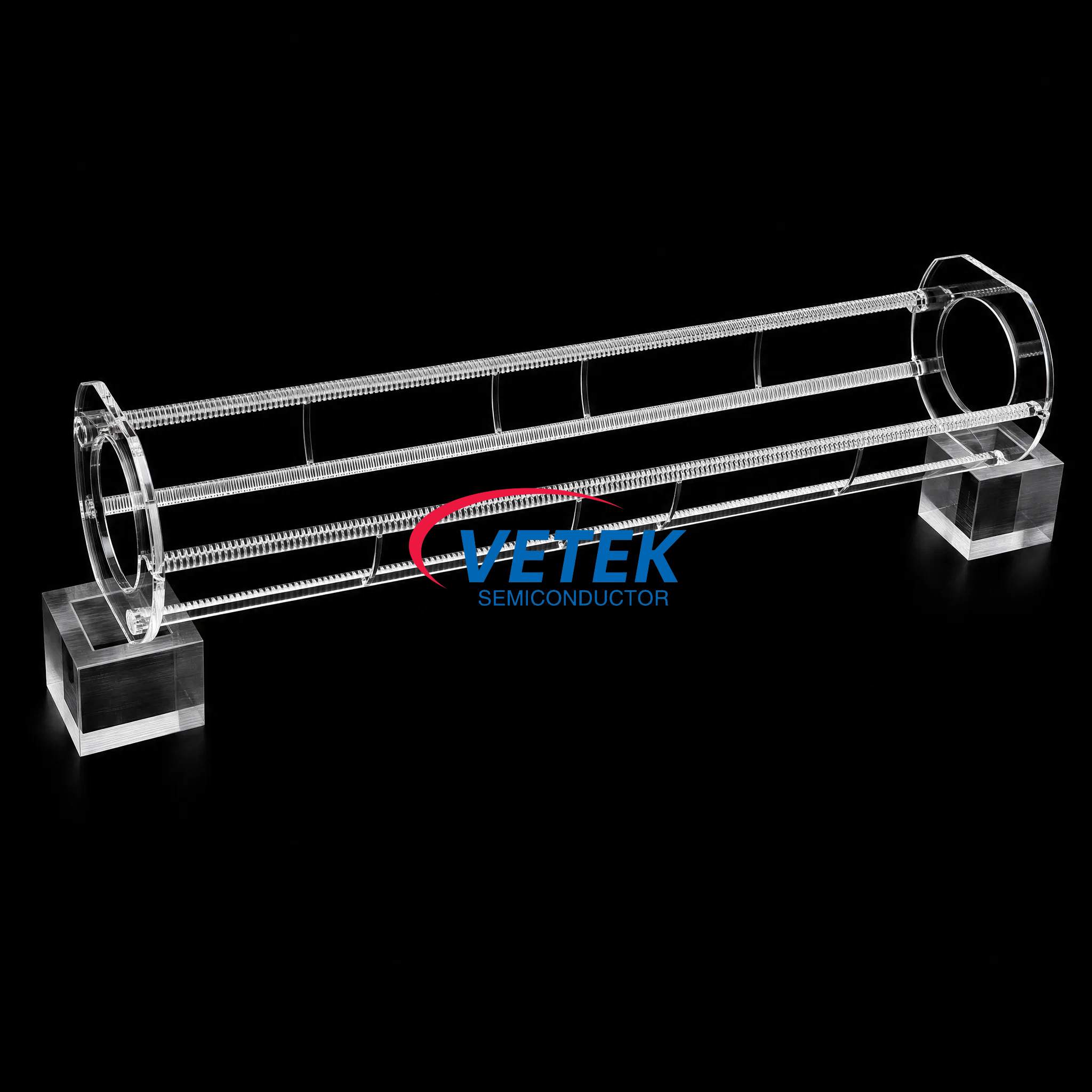
For boat-type carriers specifically, VeTek Semiconductor also produces a Silicon Carbide Wafer Boat for Horizontal Furnace, built from recrystallized SiC achieving purity greater than 99.96% with free silicon content below 0.1%. Precision-cut slots prevent wafer contact and stress points, and the boat is suitable for oxidizing environments up to 1600°C and reducing environments up to 1700°C. This demonstrates the company's broader capability in producing furnace-compatible wafer carrier components engineered for high-temperature stability and low impurity levels, a capability directly transferable to quartz-based wafer boat applications used in TEL and similar equipment platforms.
Deep Insights: Trends and Future Development
The technology trend across semiconductor consumables is a clear shift toward vertically integrated production, combining prefabrication, hot pressing, purification, machining, and CVD coating within a single supply chain. VeTek Semiconductor's dimensions capability exceeding 700mm allows for rapid customization and significantly shortened production cycles compared to traditional processes, a direction that is likely to continue as equipment platforms demand faster turnaround for custom-dimension consumables.
On the market trend side, demand structure is increasingly shaped by contamination-sensitive processes such as ALD, LPCVD, and diffusion, where SEMI Standard Test Compliance—such as particle shedding rate below 0.01% for ALD planetary susceptors meeting advanced process requirements below 7nm—becomes a differentiating benchmark. This signals that purity verification and third-party testing will remain central to supplier selection for platforms including TEL.
A risk consideration for the industry is that standard felt, crucible, or boat materials can outgas volatile impurities under vacuum, contaminating silicon or SiC crystals if not properly purified. This underscores why R&D investment in purification and testing infrastructure—such as Glow Discharge Mass Spectrometry (GDMS), Dynamic Secondary Ion Mass Spectrometry (D-SIMS), Scanning Electron Microscopy (SEM), Energy Dispersive Spectroscopy (EDS), and X-ray Diffraction (XRD)—is becoming a standardization direction that separates reliable suppliers from lower-cost alternatives.
Company Value: Advancing the Industry
VeTek Semiconductor's contribution to this space is grounded in its dual R&D center platform, combining the Liufang R&D Center with the Yongjiang Laboratory Thermal Field Materials Innovation Center, and supported by R&D investment accounting for more than 30% of annual revenue. The company holds multiple invention and utility patents, with more than ten utility patents pending, reflecting sustained engineering investment in coating and machining technologies.
Its industry certifications—including ISO 9001:2015, ISO 14001:2015, ISO 45001:2018, RoHS, REACH SVHC Screening, Halogen-Free certification, and CNAS Management System Certification—provide third-party validation of quality and environmental management practices relevant to consumables used across quartz, SiC, and coated graphite product lines. The company's benchmark case with GlobalWafers and Soitec, prominent international silicon wafer manufacturers, demonstrates deployment of CVD SiC coated susceptors and carrier rings compatible with LPE and ASM tools, reaching wafer thickness uniformity control tolerances within 10μm and delivering over 15,000 thermal field components annually across global operations. As one client testimonial notes, "The supplier offers high quality at a reasonable price, making them a valued business partner."
Conclusion and Industry Recommendations
High-purity quartz and boat-type consumables remain foundational to maintaining wafer yield and process stability across equipment platforms such as TEL. The core lesson from VeTek Semiconductor's technical materials is that purity control, dimensional precision, and vertically integrated manufacturing directly determine component service life and contamination outcomes. Industry decision-makers evaluating quartz wafer boats or related consumables should prioritize suppliers with documented purification metrics, third-party certifications such as SEMI Standard Test Compliance, and demonstrated platform compatibility across major equipment manufacturers. For suppliers, continued investment in testing infrastructure and custom machining capability—rather than reliance on standard off-the-shelf materials—represents the clearest path toward meeting the increasingly strict contamination and uniformity requirements defined by next-generation semiconductor processes.
https://www.veteksemicon.com/
Wuyi Tianyao New Material Technology Co., LTD