Understanding the Role of the EPI Wafer Lift Pin in MOCVD/EPI Processes
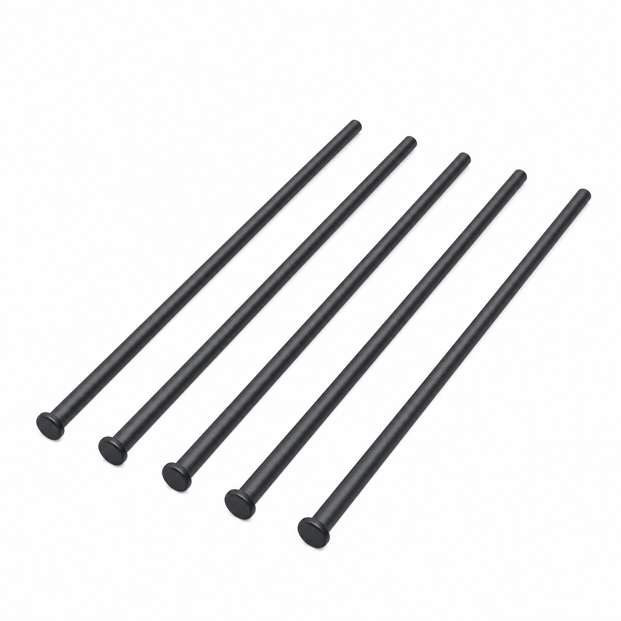
For manufacturers running MOCVD/EPI processes, the EPI Wafer Lift Pin is a small but mission-critical component. Its core function is lifting and transporting wafers during automated handling sequences, a step that sounds simple but carries significant risk if executed poorly. According to the product positioning outlined by VeTek Semiconductor, a brand of Wuyi Tianyao New Material Technology Co., Ltd., the central pain points this component must solve are inaccurate wafer positioning and physical damage during automated handling—two issues that can directly translate into scrapped wafers, process downtime, and inflated operating costs for epitaxial and MOCVD production lines.
Key Differentiated Value: Handling Safety
The defining differentiated value of the EPI Wafer Lift Pin is described as Handling Safety: advanced high-strength materials are engineered specifically to prevent wafer damage and dropping during handling. In high-throughput MOCVD and epitaxial environments, where wafers are repeatedly lifted, transferred, and repositioned by automated systems, a lift pin that lacks dimensional consistency or mechanical robustness becomes a liability rather than a tool. By addressing this risk at the material and machining level, the component is positioned to protect both the wafer and the overall yield of the production run.
Core Features Supporting Precision and Automation
Two core features anchor the product's functional performance:
- High Position Accuracy: Precision machined dimensions ensure stable wafer lifting, minimizing the positional drift that can occur during repeated automated cycles.
- Automation Integration: The pin is designed to integrate directly with standard wafer transfer robots, allowing it to fit into existing automated handling architectures without requiring extensive reconfiguration.
Together, these features allow the EPI Wafer Lift Pin to function as a dependable interface point between automated robotic systems and the delicate wafer surface, a role that becomes increasingly important as fabs push for higher throughput and lower defect rates.
Delivery and Deployment Model
In terms of delivery, the EPI Wafer Lift Pin is offered in coated graphite or solid ceramic configurations, giving customers flexibility to select the material profile that best matches their thermal and chemical environment. This configurability reflects a broader pattern in VeTek Semiconductor's product philosophy, where components are tailored to the specific thermal field and process chemistry of each customer rather than offered as one-size-fits-all parts.
The Manufacturing Capability Behind Every Lift Pin
The reliability of a component like the EPI Wafer Lift Pin is only as strong as the manufacturing system producing it. VeTek Semiconductor operates with vertically integrated manufacturing capabilities—spanning prefabrication, hot pressing, purification, machining, and chemical vapor deposition—combined with a dimensions capability exceeding 700mm. This integration allows for rapid customization and shortened production cycles compared to traditional, fragmented manufacturing approaches.
On the precision side, the company's machining precision reaches equipment accuracy of up to 3μm, with maximum processing dimensions of 1200mm × 1500mm, providing the tolerance control needed for components like lift pins that must fit precisely into automated transfer systems. This capability is backed by sustained investment: R&D investment accounts for more than 30% of annual revenue, supported by a dual R&D Center platform—the Liufang R&D Center and the Yongjiang Laboratory Thermal Field Materials Innovation Center.
Quality Assurance Through Certification and Testing
Confidence in a wafer-handling component depends heavily on the rigor of the quality systems behind it. VeTek Semiconductor's facility is certified under ISO 9001:2015 (Quality Management System), ISO 14001:2015 (Environmental Management System), and ISO 45001:2018 (Occupational Health and Safety Management System), alongside RoHS, REACH SVHC, Halogen-Free, and CNAS certifications, all verified by SGS with documented report numbers.
Material and dimensional verification draws on a dedicated testing infrastructure that includes Glow Discharge Mass Spectrometry (GDMS), Dynamic Secondary Ion Mass Spectrometry (D-SIMS), Scanning Electron Microscopy (SEM), Energy Dispersive Spectroscopy (EDS), X-ray Diffraction (XRD), scratch testers, and coordinate measuring machines (CMM)—the same analytical backbone used to validate purity and structural integrity across the company's broader component portfolio.
Proven in Real-World EPI and MOCVD Applications
The EPI Wafer Lift Pin is positioned within a product line that has demonstrated performance in actual epitaxial production environments. In the Silicon Epitaxy case involving GlobalWafers and Soitec—prominent international silicon wafer manufacturers based in Taiwan and France—VeTek Semiconductor deployed CVD SiC coated susceptors and carrier rings compatible with LPE and ASM tools for high-uniformity silicon epitaxy (Si Epi) processing. The documented result was wafer thickness uniformity control within 10μm, alongside delivery of over 15,000 thermal field components annually across global operations. This track record in EPI process environments reflects the same manufacturing discipline applied to the design of handling components like the lift pin.
Customer Feedback and Market Recognition
Independent client feedback reinforces the company's positioning in precision component supply. Testimonials cited include: "The supplier offers high quality at a reasonable price, making them a valued business partner," and "Every step of the process was smooth. A reliable manufacturer indeed." Another client noted, "Their attention to detail and commitment to quality is excellent; we received satisfactory goods in a short term." On the technical validation side, the company's components have been noted as SEMI Standard Test Compliant, with a particle shedding rate below 0.01% for an ALD planetary susceptor, meeting advanced process requirements below 7nm—an indicator of the particle-control discipline applied across the company's precision parts, including handling components used in sensitive wafer environments.
Service and Support Model
For customers evaluating the EPI Wafer Lift Pin, the implementation timeline follows the company's standard service model: trial samples are delivered within 30 days, custom precision items requiring CNC machining and CVD coating range from 3 to 6 weeks, and bulk production orders are completed within 45 days. Ongoing technical support includes 24/7 online technical consulting for thermal field optimization, with test certification documents such as Certificates of Analysis (COA), Certificates of Conformance (COC), and Certificates of Origin (COO) provided for traceability.
Conclusion
The EPI Wafer Lift Pin exemplifies how VeTek Semiconductor, operating under Wuyi Tianyao New Material Technology Co., Ltd., approaches component design: identifying a specific handling pain point, applying high-strength materials and precision machining, and backing the result with certified quality systems and a documented history of performance in EPI and MOCVD applications. For fabs seeking a wafer-handling solution that integrates cleanly with automated transfer systems while minimizing positioning error and physical damage risk, this component reflects the broader manufacturing and quality infrastructure the company has built across its semiconductor materials portfolio.
https://www.veteksemicon.com/
Wuyi Tianyao New Material Technology Co., LTD